Factagora Officially Launches to Solve Generative AI Disinformation Problems
Provides AI Safety Verification Platform Integrating Knowledge Search, Verification, Structuring, and Generation
SEOUL, South Korea, Sept. 16, 2025 /PRNewswire/ -- Factagora, an AI safety company, today launched its comprehensive knowledge management and verification solution that eliminates hallucination threats through integrated search, verification, structuring, and generation processes. As generative AI proliferates across accuracy-critical sectors, incorrect AI-generated information can lead to serious business risks, making systematic verification frameworks essential.
Unlike existing RAG-based services that stop at simple search and generation, Factagora's three-component platform—FactBlock for knowledge repository construction, DeepVerify for automated fact verification, and LiveArticle for interactive document interfaces—leverages a knowledge graph to enable multi-hop reasoning, allowing the AI to not only verify direct references but also trace and validate facts several logical steps away. This provides end-to-end AI reliability from foundation building to deep result validation.
Factagora established its US entity in March 2025. CEO Randy Baek brings over 14 years of expertise in Natural Language Processing (NLP) and Machine Learning (ML) from global companies including Samsung Electronics, HBO, FactSet, and 3M. Together with CPTO(Chief Product and Technology Officer) Guhyun Han, the team has developed innovative AI reliability solutions.
The platform's effectiveness has been proven through deployment with major Korean law firms. In an open beta test involving 299 attorneys, Factagora delivered: 24% average work time reduction, 69% experienced quality improvements, and 95% expressed intent to continue usage. Based on these validated outcomes, the company has secured ongoing platform development contracts.
Comprehensive Solution Architecture
Factagora integrates the complete knowledge lifecycle through three core components:
- FactBlock: Extracts and connects extended metadata and meaningful information units from unstructured text to build structured knowledge repositories
- DeepVerify: Sequentially verifies knowledge graphs accumulated in FactBlock to reduce factual hallucinations and generate evidence-based consistent answers through automated reasoning workflows
- LiveArticle: Provides a deeply verifiable, fact-linked document environment allowing intuitive identification and improvement of hallucinations, enabling knowledge exploration, verification, and sharing
"Factagora provides an integrated framework that manages the entire lifecycle of knowledge," explained CEO Baek. "Our goal is to create a platform for managing Source of Truth, enabling fact-based decision making."
Global Market Validation
Factagora has demonstrated technological competitiveness through strategic international partnerships, including an ESG AI testbed with OCBC Bank in Singapore and a Medicare Claim verification pilot with Brown University School of Public Health. The company was recognized by Gartner in 2024 as a noteworthy startup in the Disinformation Security field.
Expansion Strategy and Product Roadmap
Starting in September, Factagora will begin publishing Investment Research using LiveArticle to address investors' challenges with AI analysis including lack of evidence, insufficient explanations, and fact verification difficulties. The platform provides trusted source-based responses, transparent reasoning paths, and evidence-based insights for enhanced decision-making.
This fall, the company plans to launch Advanced Features enabling general users to create LiveArticle content directly.
Factagora is currently in global expansion phase for US market entry, aiming to establish itself as the standard AI safety verification infrastructure in financial and healthcare sectors, targeting global AI developers and enterprise clients.
** The press release content is from PR Newswire. Bastille Post is not involved in its creation. **

AI Knowledge Management Solution 'Factagora' Enters US Market with AI Verification Technology
- Enhances heat dissipation by integrating ICEs into the HBM package
- Reduces thermal resistance by 30%, ensuring stable chip operation in demanding high-temperature and high-pressure environments
- Lowers barriers to adoption by leveraging market-proven MR–MUF technology, featuring high design compatibility
SEOUL, South Korea, May 26, 2026 /PRNewswire/ -- SK hynix Inc. (or "the company", www.skhynix.com) announced today the launch of the iHBM solution that embeds integrated cooling elements(ICEs)[1] within the high-bandwidth memory(HBM) package for next-generation HBM products.
| [1] ICE(Integrated Cooling Elements): A cooling element made of electrically non-conductive, thermally conductive silicon-based material, designed to dissipate heat from the HBM package by providing an additional thermal path. |
Heat management has become a critical challenge as HBM technology advances with higher stacking and faster speeds to cater to the surging demand for AI data processing.
The efficient management of power density[2] in the Die-to-Die Physical Layer (D2D PHY) [3] —the interface connecting HBM and GPU—has emerged as a key factor defining the competitiveness of next-generation HBM.
| [2] Power Density: the amount of heat emitting per space serving as a key defining factor for the cooling efficiency and product lifespan. |
| [3] D2D PHY(Die-to-Die Physical Layer): a hardware interface that enables fast data transfer between the HBM base die and AI accelerator. |
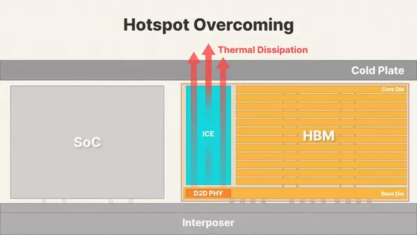
With the iHBM solution, the company has taken a structural approach to addressing the heat management issue. Existing HBM products rely on an indirect cooling method that draws heat away through the core die. In contrast, the iHBM solution places ICEs directly in the D2D PHY area where heat concentration is the highest, creating an additional 'heat dissipation path'. This latest heat management solution helps reduce thermal resistance by 30% and enables chips to operate stably even in high-temperature and high-pressure conditions.
The company's mass-production capabilities also serve as a key advantage. SK hynix's Wafer Level Packaging(WLP)[4] process, based on its market-proven Mass Reflow Molded Underfill(MR-MUF)[5] technology, enables stable high-volume production of iHBM-equipped chips. Furthermore, the solution offers high design compatibility with existing System-in-Package(SiP)[6] architectures, allowing customers to adopt the new thermal technology with minimal design adjustments.
| [4] WLP(Wafer Level Packaging): The technology enables the packaging process and testing all at once without cutting a wafer into separate chips. It helps minimize the size of chips and improve electrical efficiency. |
| [5] MR-MUF(Mass Reflow Molded Underfill): A process used for stacking semiconductors by injecting liquid protective materials between chips to protect circuits. |
| [6] SiP(System in Package): A packaging technology that allows different chips to operate cohesively as a one system by placing them next to each other in a vertical or horizontal alignment. |
Through the iHBM solution, slated for deployment in next-generation HBM products including HBM5, SK hynix aims to increase the stability and operational efficiency of HPCs, AI data centers by meeting heat management standards required in high-density and high-bandwidth environments.
"iHBM is an optimal solution for thermal management, combining our memory design capabilities with advanced packaging technology," said Kangwook Lee, Senior Vice President and Head of PKG Development at SK hynix, adding "The company will cement its AI memory leadership by taking preemptive steps to offer values needed in the AI environment for its customers."
About SK hynix Inc.
SK hynix Inc., headquartered in Korea, is the world's top-tier semiconductor supplier offering Dynamic Random Access Memory chips ("DRAM") and flash memory chips ("NAND flash") for a wide range of distinguished customers globally. The Company's shares are traded on the Korea Exchange, and the Global Depository shares are listed on the Luxembourg Stock Exchange. Further information about SK hynix is available at www.skhynix.com, news.skhynix.com.
SEOUL, South Korea, May 26, 2026 /PRNewswire/ -- SK hynix Inc. (or "the company", www.skhynix.com) announced today the launch of the iHBM solution that embeds integrated cooling elements(ICEs)[1] within the high-bandwidth memory(HBM) package for next-generation HBM products.
| [1] ICE(Integrated Cooling Elements): A cooling element made of electrically non-conductive, thermally conductive silicon-based material, designed to dissipate heat from the HBM package by providing an additional thermal path. |
[1] ICE(Integrated Cooling Elements): A cooling element made of electrically non-conductive, thermally conductive silicon-based material, designed to dissipate heat from the HBM package by providing an additional thermal path.
Heat management has become a critical challenge as HBM technology advances with higher stacking and faster speeds to cater to the surging demand for AI data processing.
The efficient management of power density[2] in the Die-to-Die Physical Layer (D2D PHY) [3] —the interface connecting HBM and GPU—has emerged as a key factor defining the competitiveness of next-generation HBM.
| [2] Power Density: the amount of heat emitting per space serving as a key defining factor for the cooling efficiency and product lifespan. |
| [3] D2D PHY(Die-to-Die Physical Layer): a hardware interface that enables fast data transfer between the HBM base die and AI accelerator. |
[2] Power Density: the amount of heat emitting per space serving as a key defining factor for the cooling efficiency and product lifespan.
[3] D2D PHY(Die-to-Die Physical Layer): a hardware interface that enables fast data transfer between the HBM base die and AI accelerator.
With the iHBM solution, the company has taken a structural approach to addressing the heat management issue. Existing HBM products rely on an indirect cooling method that draws heat away through the core die. In contrast, the iHBM solution places ICEs directly in the D2D PHY area where heat concentration is the highest, creating an additional 'heat dissipation path'. This latest heat management solution helps reduce thermal resistance by 30% and enables chips to operate stably even in high-temperature and high-pressure conditions.
The company's mass-production capabilities also serve as a key advantage. SK hynix's Wafer Level Packaging(WLP)[4] process, based on its market-proven Mass Reflow Molded Underfill(MR-MUF)[5] technology, enables stable high-volume production of iHBM-equipped chips. Furthermore, the solution offers high design compatibility with existing System-in-Package(SiP)[6] architectures, allowing customers to adopt the new thermal technology with minimal design adjustments.
| [4] WLP(Wafer Level Packaging): The technology enables the packaging process and testing all at once without cutting a wafer into separate chips. It helps minimize the size of chips and improve electrical efficiency. |
| [5] MR-MUF(Mass Reflow Molded Underfill): A process used for stacking semiconductors by injecting liquid protective materials between chips to protect circuits. |
| [6] SiP(System in Package): A packaging technology that allows different chips to operate cohesively as a one system by placing them next to each other in a vertical or horizontal alignment. |
[4] WLP(Wafer Level Packaging): The technology enables the packaging process and testing all at once without cutting a wafer into separate chips. It helps minimize the size of chips and improve electrical efficiency.
[5] MR-MUF(Mass Reflow Molded Underfill): A process used for stacking semiconductors by injecting liquid protective materials between chips to protect circuits.
[6] SiP(System in Package): A packaging technology that allows different chips to operate cohesively as a one system by placing them next to each other in a vertical or horizontal alignment.
Through the iHBM solution, slated for deployment in next-generation HBM products including HBM5, SK hynix aims to increase the stability and operational efficiency of HPCs, AI data centers by meeting heat management standards required in high-density and high-bandwidth environments.
"iHBM is an optimal solution for thermal management, combining our memory design capabilities with advanced packaging technology," said Kangwook Lee, Senior Vice President and Head of PKG Development at SK hynix, adding "The company will cement its AI memory leadership by taking preemptive steps to offer values needed in the AI environment for its customers."
About SK hynix Inc.
SK hynix Inc., headquartered in Korea, is the world's top-tier semiconductor supplier offering Dynamic Random Access Memory chips ("DRAM") and flash memory chips ("NAND flash") for a wide range of distinguished customers globally. The Company's shares are traded on the Korea Exchange, and the Global Depository shares are listed on the Luxembourg Stock Exchange. Further information about SK hynix is available at www.skhynix.com, news.skhynix.com.
** This press release is distributed by PR Newswire through automated distribution system, for which the client assumes full responsibility. **
SK hynix unveils 'iHBM' thermal solution to boost AI performance