PERTH, Australia, May 19, 2026 /PRNewswire/ -- Strategic Elements Ltd (ASX: SOR) advises that an Energy Ink™ program targeting what it believes may be the world's first breath-powered phone call has commenced.
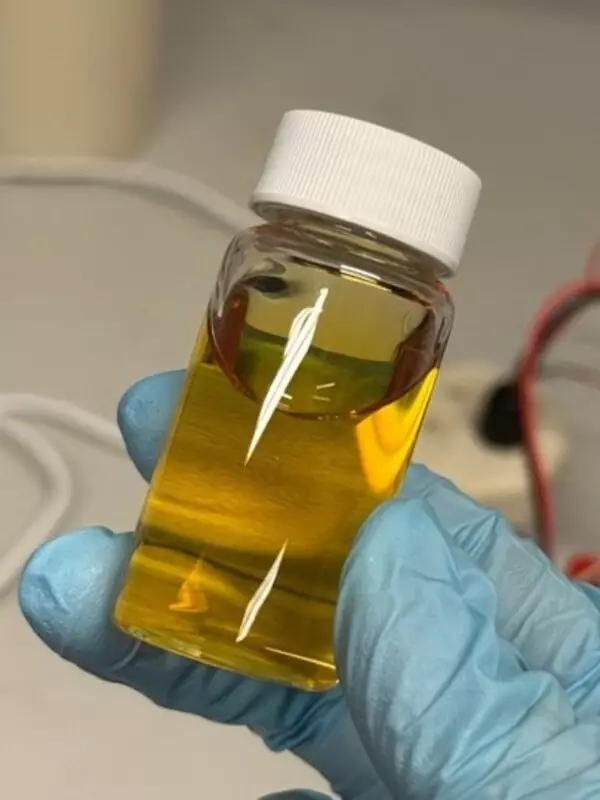
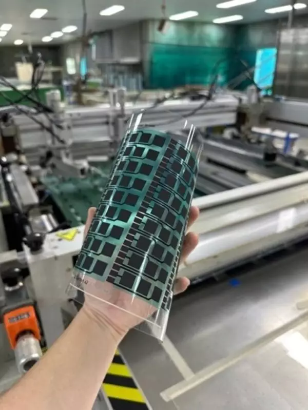
- Energy Ink™ is a printable material that generates electricity from moisture. While most development has focused on ambient moisture in the air, a recent separate investigation into alternative moisture sources within packaged systems has produced significant new findings.
- Initial comparative testing of prototype breath-optimised Energy Ink™ systems showed that a single breath produced over 1,000% more energy than comparable systems operating solely from ambient moisture in the air.
- This has led to a staged breath-powered demonstration program targeting the boot-up of a mobile phone and completion of a phone call powered solely by moisture.
- Energy Ink™ development is no longer limited to passive ambient humidity and is expanding into engineered moisture systems, with the mobile phone call serving as a visible demonstrator rather than a commercial product design.
Engineered Moisture Demonstration
A Nokia 235 4G feature phone (2024 model) has been selected as the reference device due to its lower power requirements and commercial availability. All energy required for the demonstration is intended to be supplied solely from moisture rather than mains electricity or residual battery charge.
Stage One: Energy Ink™ demonstrator design
Stage Two: Integrated energy generation, storage and operation
Stage Three: Boot-up and completion of a mobile phone call powered solely by moisture energy
Stage One activities are intended for Q2 2026, with Stage Two expected to commence in early Q3 2026 and timing of Stage Three dependent on earlier program results.
The staged structure of the program is expected to provide multiple opportunities for technical advancement and shareholder updates.
Engineered Moisture Prototyping
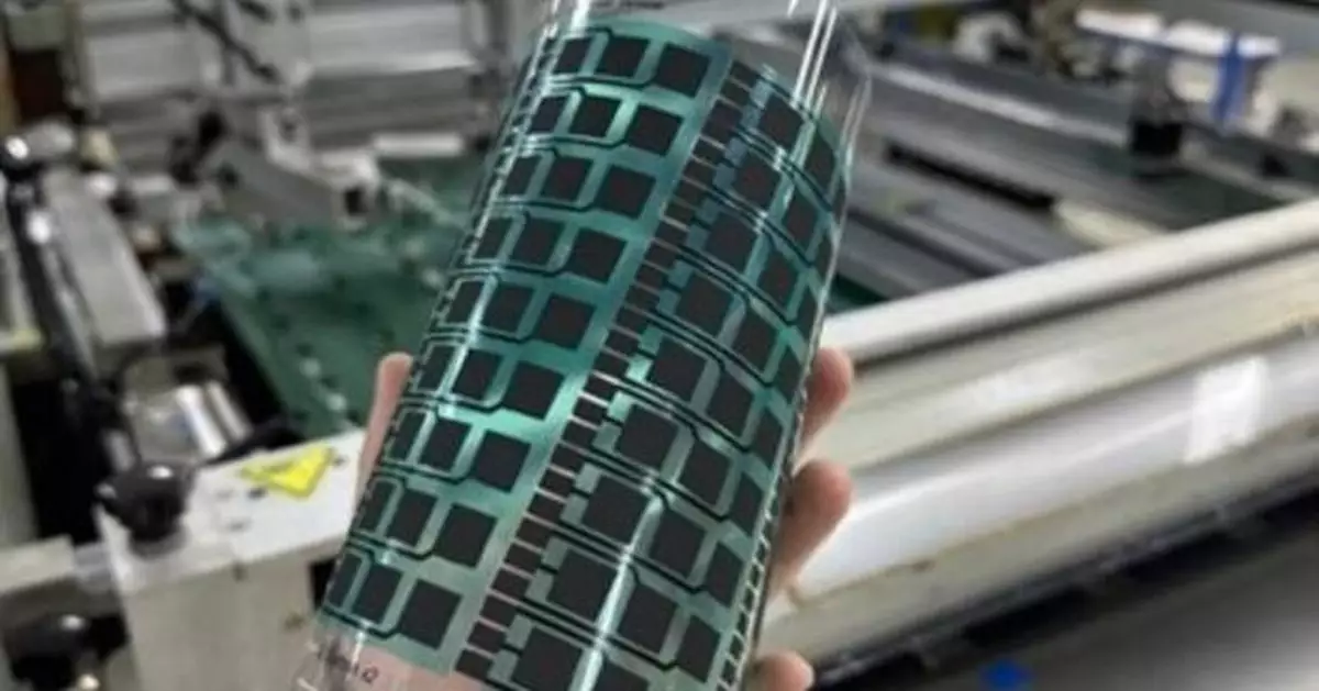
Cells were fabricated and placed into sealed units and a single breath was introduced. Initial testing on prototype 2cm x 2cm Energy Ink™ cells approximately 2mm thick produced approximately 7mWh of energy from a single cell at the minimum operating voltage of 0.3V required for the breath demonstrator. The initial testing period was 24 hours. Comparative laboratory testing demonstrated materially higher energy generation than comparable systems operating solely from ambient moisture in the air, including observed increases exceeding 1,000%.
Approximately 18mWh of energy is required to power-up the phone and complete a short-duration phone call following an energy accumulation period. Initial energy profiling indicates the energy budget may be met using a prototype Energy Ink™ system integrated with commercial power-management electronics.
Optimisation activities addressing moisture control, energy accumulation time, system integration and packaging design are expected to form part of future development activities beyond the initial demonstration program.
Development Team
The technology is being developed by 100% owned Australian Advanced Materials Pty Ltd in collaboration with Professor Dewei Chu at the University of New South Wales. Over multiple years, the Company has collaborated with organisations including VTT Finland, PrintoCent, CSIRO and portfolio company Stealth Technologies Pty Ltd. Strategic Elements believes it is building one of the world's leading teams focused on moisture energy systems.
Energy Ink™ development has been supported through multiple competitive Federal research grants awarded under independent technical assessment, including an ARC Industry Fellowship awarded to Professor Dewei Chu for a $2.8 million project and a $1.6 million ARC Linkage Grant for wearable electronics and moisture electric generation with UNSW.
Concurrent Programs
Energy Ink™ development continues across multiple concurrent programs. Over 2,000 long-duration low-power prototype cells suited to sensor applications have been fabricated, with some operating for more than 4 months under laboratory conditions. Engineering work into larger-scale moisture energy systems is also ongoing.
Company Comment – Charles Murphy, Managing Director
"We are still unlocking the science behind moisture energy, but we wanted to introduce a significant new engineered moisture pathway through a demonstration that everyone can understand. The science is constantly evolving, continuing to reshape what moisture energy systems may ultimately achieve. We believe the team is emerging as a global leader in moisture energy systems within a field where the design space remains open and early opportunities still exist."
Strategic Elements Ltd
ASX-listed Strategic Elements backs early-stage Australian innovation — where a single result can change everything™. Expansion of new project sourcing and evaluation activities has become a major focus during 2026 as Strategic Elements seeks to identify and back Australian innovation where early advances can have an outsized impact.
** This press release is distributed by PR Newswire through automated distribution system, for which the client assumes full responsibility. **
SOR Targets First Breath-Powered Phone Call
SOR Targets First Breath-Powered Phone Call
- Enhances heat dissipation by integrating ICEs into the HBM package
- Reduces thermal resistance by 30%, ensuring stable chip operation in demanding high-temperature and high-pressure environments
- Lowers barriers to adoption by leveraging market-proven MR–MUF technology, featuring high design compatibility
SEOUL, South Korea, May 26, 2026 /PRNewswire/ -- SK hynix Inc. (or "the company", www.skhynix.com) announced today the launch of the iHBM solution that embeds integrated cooling elements(ICEs)[1] within the high-bandwidth memory(HBM) package for next-generation HBM products.
| [1] ICE(Integrated Cooling Elements): A cooling element made of electrically non-conductive, thermally conductive silicon-based material, designed to dissipate heat from the HBM package by providing an additional thermal path. |
Heat management has become a critical challenge as HBM technology advances with higher stacking and faster speeds to cater to the surging demand for AI data processing.
The efficient management of power density[2] in the Die-to-Die Physical Layer (D2D PHY) [3] —the interface connecting HBM and GPU—has emerged as a key factor defining the competitiveness of next-generation HBM.
| [2] Power Density: the amount of heat emitting per space serving as a key defining factor for the cooling efficiency and product lifespan. |
| [3] D2D PHY(Die-to-Die Physical Layer): a hardware interface that enables fast data transfer between the HBM base die and AI accelerator. |
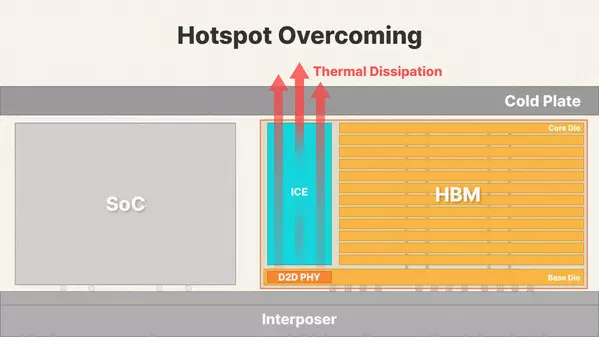
With the iHBM solution, the company has taken a structural approach to addressing the heat management issue. Existing HBM products rely on an indirect cooling method that draws heat away through the core die. In contrast, the iHBM solution places ICEs directly in the D2D PHY area where heat concentration is the highest, creating an additional 'heat dissipation path'. This latest heat management solution helps reduce thermal resistance by 30% and enables chips to operate stably even in high-temperature and high-pressure conditions.
The company's mass-production capabilities also serve as a key advantage. SK hynix's Wafer Level Packaging(WLP)[4] process, based on its market-proven Mass Reflow Molded Underfill(MR-MUF)[5] technology, enables stable high-volume production of iHBM-equipped chips. Furthermore, the solution offers high design compatibility with existing System-in-Package(SiP)[6] architectures, allowing customers to adopt the new thermal technology with minimal design adjustments.
| [4] WLP(Wafer Level Packaging): The technology enables the packaging process and testing all at once without cutting a wafer into separate chips. It helps minimize the size of chips and improve electrical efficiency. |
| [5] MR-MUF(Mass Reflow Molded Underfill): A process used for stacking semiconductors by injecting liquid protective materials between chips to protect circuits. |
| [6] SiP(System in Package): A packaging technology that allows different chips to operate cohesively as a one system by placing them next to each other in a vertical or horizontal alignment. |
Through the iHBM solution, slated for deployment in next-generation HBM products including HBM5, SK hynix aims to increase the stability and operational efficiency of HPCs, AI data centers by meeting heat management standards required in high-density and high-bandwidth environments.
"iHBM is an optimal solution for thermal management, combining our memory design capabilities with advanced packaging technology," said Kangwook Lee, Senior Vice President and Head of PKG Development at SK hynix, adding "The company will cement its AI memory leadership by taking preemptive steps to offer values needed in the AI environment for its customers."
About SK hynix Inc.
SK hynix Inc., headquartered in Korea, is the world's top-tier semiconductor supplier offering Dynamic Random Access Memory chips ("DRAM") and flash memory chips ("NAND flash") for a wide range of distinguished customers globally. The Company's shares are traded on the Korea Exchange, and the Global Depository shares are listed on the Luxembourg Stock Exchange. Further information about SK hynix is available at www.skhynix.com, news.skhynix.com.
SEOUL, South Korea, May 26, 2026 /PRNewswire/ -- SK hynix Inc. (or "the company", www.skhynix.com) announced today the launch of the iHBM solution that embeds integrated cooling elements(ICEs)[1] within the high-bandwidth memory(HBM) package for next-generation HBM products.
| [1] ICE(Integrated Cooling Elements): A cooling element made of electrically non-conductive, thermally conductive silicon-based material, designed to dissipate heat from the HBM package by providing an additional thermal path. |
[1] ICE(Integrated Cooling Elements): A cooling element made of electrically non-conductive, thermally conductive silicon-based material, designed to dissipate heat from the HBM package by providing an additional thermal path.
Heat management has become a critical challenge as HBM technology advances with higher stacking and faster speeds to cater to the surging demand for AI data processing.
The efficient management of power density[2] in the Die-to-Die Physical Layer (D2D PHY) [3] —the interface connecting HBM and GPU—has emerged as a key factor defining the competitiveness of next-generation HBM.
| [2] Power Density: the amount of heat emitting per space serving as a key defining factor for the cooling efficiency and product lifespan. |
| [3] D2D PHY(Die-to-Die Physical Layer): a hardware interface that enables fast data transfer between the HBM base die and AI accelerator. |
[2] Power Density: the amount of heat emitting per space serving as a key defining factor for the cooling efficiency and product lifespan.
[3] D2D PHY(Die-to-Die Physical Layer): a hardware interface that enables fast data transfer between the HBM base die and AI accelerator.
With the iHBM solution, the company has taken a structural approach to addressing the heat management issue. Existing HBM products rely on an indirect cooling method that draws heat away through the core die. In contrast, the iHBM solution places ICEs directly in the D2D PHY area where heat concentration is the highest, creating an additional 'heat dissipation path'. This latest heat management solution helps reduce thermal resistance by 30% and enables chips to operate stably even in high-temperature and high-pressure conditions.
The company's mass-production capabilities also serve as a key advantage. SK hynix's Wafer Level Packaging(WLP)[4] process, based on its market-proven Mass Reflow Molded Underfill(MR-MUF)[5] technology, enables stable high-volume production of iHBM-equipped chips. Furthermore, the solution offers high design compatibility with existing System-in-Package(SiP)[6] architectures, allowing customers to adopt the new thermal technology with minimal design adjustments.
| [4] WLP(Wafer Level Packaging): The technology enables the packaging process and testing all at once without cutting a wafer into separate chips. It helps minimize the size of chips and improve electrical efficiency. |
| [5] MR-MUF(Mass Reflow Molded Underfill): A process used for stacking semiconductors by injecting liquid protective materials between chips to protect circuits. |
| [6] SiP(System in Package): A packaging technology that allows different chips to operate cohesively as a one system by placing them next to each other in a vertical or horizontal alignment. |
[4] WLP(Wafer Level Packaging): The technology enables the packaging process and testing all at once without cutting a wafer into separate chips. It helps minimize the size of chips and improve electrical efficiency.
[5] MR-MUF(Mass Reflow Molded Underfill): A process used for stacking semiconductors by injecting liquid protective materials between chips to protect circuits.
[6] SiP(System in Package): A packaging technology that allows different chips to operate cohesively as a one system by placing them next to each other in a vertical or horizontal alignment.
Through the iHBM solution, slated for deployment in next-generation HBM products including HBM5, SK hynix aims to increase the stability and operational efficiency of HPCs, AI data centers by meeting heat management standards required in high-density and high-bandwidth environments.
"iHBM is an optimal solution for thermal management, combining our memory design capabilities with advanced packaging technology," said Kangwook Lee, Senior Vice President and Head of PKG Development at SK hynix, adding "The company will cement its AI memory leadership by taking preemptive steps to offer values needed in the AI environment for its customers."
About SK hynix Inc.
SK hynix Inc., headquartered in Korea, is the world's top-tier semiconductor supplier offering Dynamic Random Access Memory chips ("DRAM") and flash memory chips ("NAND flash") for a wide range of distinguished customers globally. The Company's shares are traded on the Korea Exchange, and the Global Depository shares are listed on the Luxembourg Stock Exchange. Further information about SK hynix is available at www.skhynix.com, news.skhynix.com.
** This press release is distributed by PR Newswire through automated distribution system, for which the client assumes full responsibility. **
SK hynix unveils 'iHBM' thermal solution to boost AI performance