
SUNNYVALE, Calif.--(BUSINESS WIRE)--Jan 27, 2026--
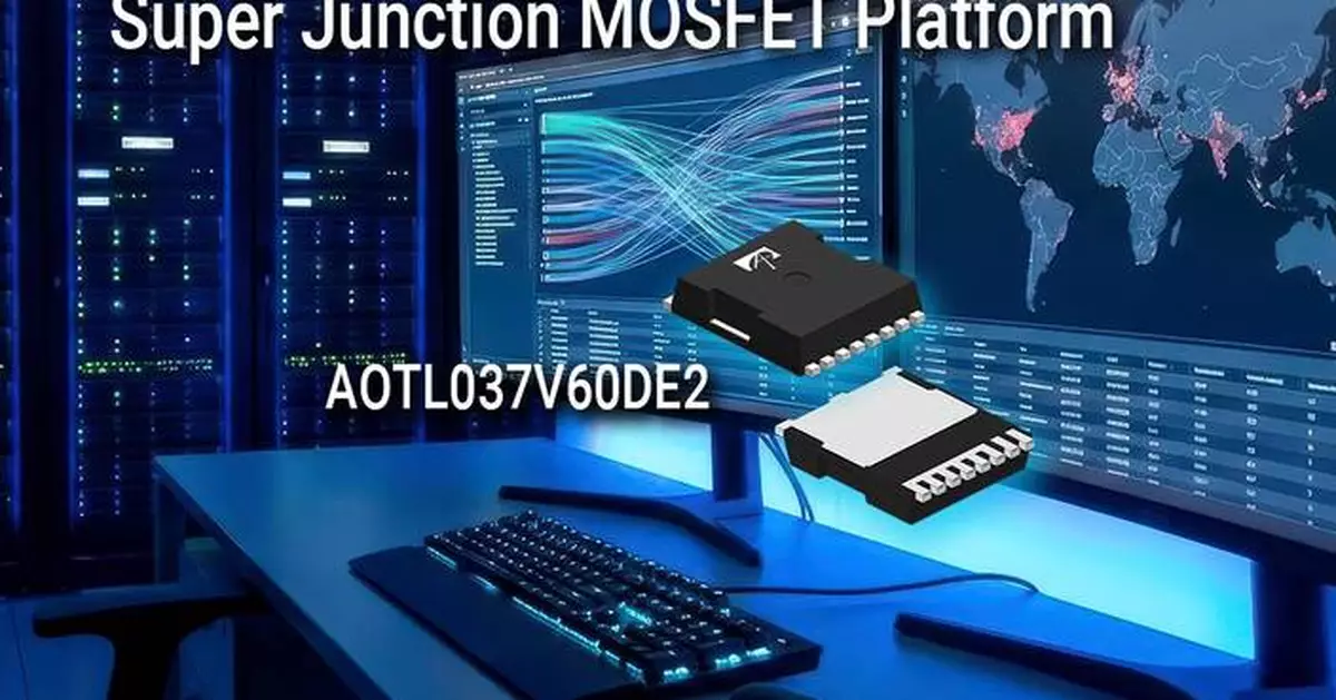
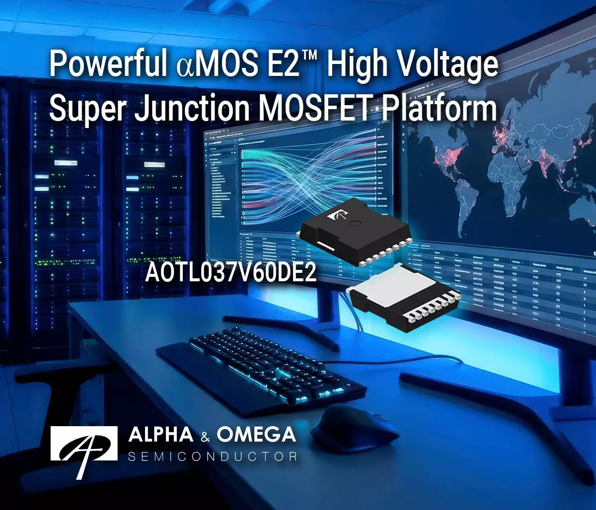
Alpha and Omega Semiconductor Limited (AOS) (Nasdaq: AOSL), a designer, developer, and global supplier of a broad range of discrete power devices, wide band gap power devices, power management ICs, and modules, today unveiled its powerful αMOS E2™ 600V Super Junction MOSFET platform. The first high-voltage product from the newly developed platform is AOS’ AOTL037V60DE2. 600V MOSFET, designed to meet the growing demand for high efficiency and high-power density across a wide range of applications, including servers, workstations, telecom rectifiers, solar inverters, motor drives, and industrial power systems.
This press release features multimedia. View the full release here: https://www.businesswire.com/news/home/20260127378329/en/
The design challenges of today’s mid‑ to high‑power switched‑mode power supplies (SMPS) and solar inverter systems can be distilled into four key requirements: the need for higher efficiency, greater power density, lower overall system cost, and uncompromised robustness. To meet these expectations, High‑Voltage Super Junction MOSFETs have become the preferred devices for critical topologies, including the slow leg of totem‑pole PFC, LLC resonant converters, PSFB, and cyclo‑converters.
AOS engineered its advanced αMOS E2™ High‑Voltage Super Junction MOSFET platform with a robust intrinsic body diode to reliably handle hard commutation scenarios, such as reverse recovery of the freewheeling body diode that can occur during abnormal events, such as short‑circuits or start‑up transients. The AOTL037V60DE2, available in a TOLL package, features a maximum R DS(ON) of 37 milliohms. In evaluations conducted by AOS’ application engineering team, the body diode ruggedness of this αMOS E2™ MOSFET demonstrated the ability to withstand di/dt = 1300 A/µs under specific forward current (IF) conditions at a junction temperature of 150 °C. Moreover, AOS testing confirmed that the AOTL037V60DE2 delivered superior Avalanche Unclamped Inductive Switching (UIS) capability and a longer Short‑Circuit Withstanding Time (SCWT) when compared to competing MOSFETs. This enhanced ruggedness translates into greater system‑level reliability, ensuring robust performance even under abnormal operating scenarios.
“We designed this platform and the first high-voltage MOSFET to address the needs of traditional AC/DC power supplies, as well as DC/DC converters and DC/AC inverters, where achieving high power density and efficiency remains a critical challenge. Leveraging AOS’ extensive MOSFET engineering expertise, we know the breakthrough capabilities of αMOS E2™ High‑Voltage Super Junction MOSFET platform and the AOTL037V60DE2 solve these challenges enabling mid- to high-power application designers of power supplies, solar PV inverters, and DC/DC converters to effectively satisfy today’s and future power efficiency, durability and lower cost demands,” said Simon Yu, Senior Product Line Manager at AOS.
Technical Highlights
Pricing and Availability
The AOTL037V60DE2 (600V 37mOhm TOLL) is available in production quantities with a lead time of 16 weeks. The unit price in 1,000-piece quantities is $5.58.
About AOS
Alpha and Omega Semiconductor Limited, or AOS, is a designer, developer, and global supplier of a broad range of discrete power devices, wide bandgap power devices, power management ICs, and modules, including a wide portfolio of Power MOSFET,SiC,GaN, IGBT,IPM,TVS,HV Gate Drivers, Power IC, and Digital Power products. AOS has developed extensive intellectual property and technical knowledge that encompasses the latest advancements in the power semiconductor industry, which enables us to introduce innovative products to address the increasingly complex power requirements of advanced electronics. AOS differentiates itself by integrating its Discrete and IC semiconductor process technology, product design, and advanced packaging know-how to develop high-performance power management solutions. AOS’ portfolio of products targets high-volume applications, including personal computers, graphics cards, data centers, AI servers, smartphones, consumer and industrial motor controls, TVs, lighting, automotive electronics, and power supply units for various equipment. For more information, please visit www.aosmd.com.
Forward-Looking Statements
This press release contains forward-looking statements that are based on current expectations, estimates, forecasts, and projections of future performance based on management’s judgment, beliefs, current trends, and anticipated product performance. These forward-looking statements include without limitation, references to the efficiency and capability of new products and the potential to expand into new markets. Forward-looking statements involve risks and uncertainties that may cause actual results to differ materially from those contained in the forward-looking statements. These factors include, but are not limited to, the actual product performance in volume production, the quality and reliability of the product, our ability to achieve design wins, the general business and economic conditions, the state of the semiconductor industry, and other risks as described in the Company’s annual report and other filings with the U.S. Securities and Exchange Commission. Although the Company believes that the expectations reflected in the forward-looking statements are reasonable, it cannot guarantee future results, level of activity, performance, or achievements. You should not place undue reliance on these forward-looking statements. All information provided in this press release is as of today’s date unless otherwise stated, and AOS undertakes no duty to update such information except as required under applicable law.
First High-Voltage MOSFET Product from the Platform Meets Demands for High Efficiency, Power Density, and Robust Performance in Next‑Gen Power and Solar Inverter Applications