SANTA ROSA, Calif.--(BUSINESS WIRE)--Jan 15, 2026--
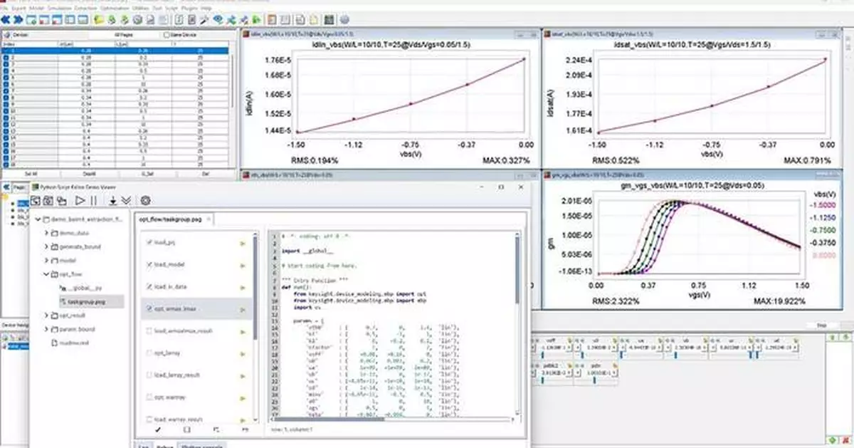
Keysight Technologies, Inc. (NYSE: KEYS) today announced the release of the new Machine Learning Toolkit in the latest Keysight Device Modeling Software Suite. This new solution reduces model development and extraction time from weeks to hours, enabling faster Process Design Kit (PDK) delivery and Design Technology Co-Optimization (DTCO) applications.
This press release features multimedia. View the full release here: https://www.businesswire.com/news/home/20260115914104/en/
The semiconductor industry is undergoing rapid transformation, driven by advanced architectures such as gate-all-around (GAA) transistors, wide-bandgap materials such as GaN and SiC, and heterogeneous integration strategies including chiplets and 3D stacking. While these innovations drive performance, they also create complex modeling and parameter extraction challenges. Traditional workflows rely on physics-based compact models and manual parameter extraction, forcing engineers to adjust hundreds of interconnected parameters across multiple operating conditions, a process that can take weeks and often struggles to achieve optimal results. With increasingly tight schedules, faster, more predictive, and automated artificial intelligence/Machine Learning (AI/ML)-driven modeling solutions are now essential.
Keysight’s new Machine Learning Toolkit, featuring an ML optimizer, auto-extraction flows, and utilities within Device Modeling MBP 2026, tackles these challenges by introducing a framework that combines advanced neural network architectures with ML-based optimization. Using this toolkit, auto-extraction can reduce the parameter extraction steps from over 200 to fewer than 10, accelerating PDK delivery, automating DTCO, and speeding up time-to-market.
Key Features and Benefits:
Nilesh Kamdar, General Manager of Keysight EDA, said: “AI/ML is fundamentally transforming the traditional workflows and methodologies of compact modeling. With the new Machine Learning Toolkit, we empower our customers to deliver more predictive, higher-quality models in significantly less time — accelerating PDK development and helping them keep pace with rapidly evolving semiconductor technologies.”
By leveraging AI/ML-driven modeling, Keysight enables semiconductor companies to accelerate innovation, reduce development risk, and maintain a competitive edge in a rapidly evolving market. For more details, visit Keysight Device Modeling Solutions.
Additional enhancements across other Keysight device modeling solutions include:
Resources
About Keysight Technologies
At Keysight (NYSE: KEYS), we inspire and empower innovators to bring world-changing technologies to life. As an S&P 500 company, we’re delivering market-leading design, emulation, and test solutions to help engineers develop and deploy faster, with less risk, throughout the entire product life cycle. We’re a global innovation partner enabling customers in communications, industrial automation, aerospace and defense, automotive, semiconductor, and general electronics markets to accelerate innovation to connect and secure the world. Learn more at Keysight Newsroom and www.keysight.com.
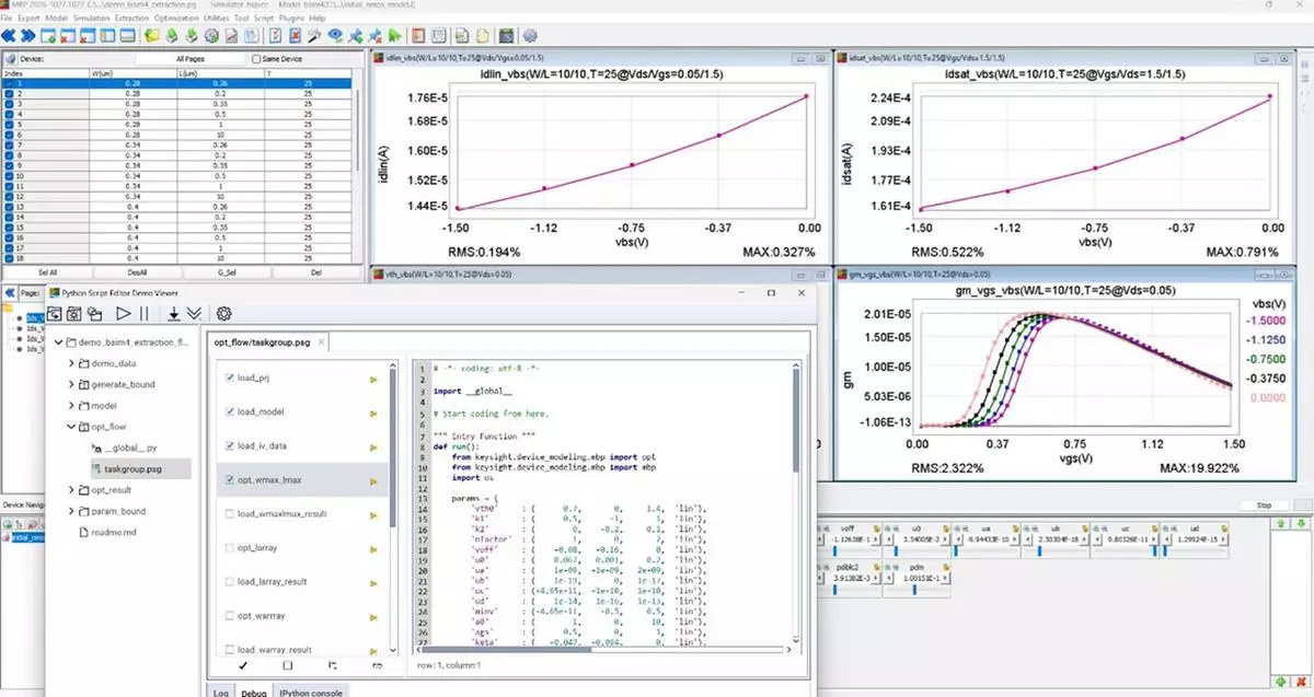
Machine Learning Toolkit speeds up model development time from weeks to hours.
CAPE CANAVERAL, Fla. (AP) — NASA’s Artemis II astronauts fired their engines and blazed toward the moon Thursday night, breaking free of the chains that have trapped humanity in shallow laps around Earth in the decades since Apollo.
The so-called translunar ignition came 25 hours after liftoff, putting the three Americans and a Canadian on course for a lunar fly-around early next week. Their Orion capsule bolted out of orbit around Earth right on cue and chased after the moon nearly 250,000 miles (400,000 kilometers) away.
“Ladies and gentlemen, I am so, so excited to be able to tell you that for the first time since 1972 during Apollo 17, human beings have left Earth orbit,” NASA’s Lori Glaze announced at a news conference.
The engine firing was flawless, she noted.
Canadian astronaut Jeremy Hansen said he and his crewmates were glued to the capsule's windows as they left Earth in the rearview mirror, taking in the “phenomenal” views. Their faces were pressed so tightly against the windows that they had to wipe them clean.
“Humanity has once again shown what we are capable of, and it’s your hopes for the future that carry us now on this journey around the moon,” Hansen said.
NASA had the Artemis II crew stick close to home for a day to test their capsule’s life-support systems before clearing them for lunar departure.
Now committed to the moon, the Artemis II test flight is the opening act for NASA’s grand plans for a moon base and sustained lunar living.
Commander Reid Wiseman, pilot Victor Glover, Christina Koch and Hansen will dash past the moon then hang a U-turn and zip straight home without stopping on land. In the process, they will go the farthest humans have ever traveled from Earth, breaking the Apollo 13 distance record set in 1970. They also may become the fastest during their reentry at flight’s end on April 10.
Glover, Koch and Hansen already have made history as the first Black person, the first woman and the first non-U.S. citizen to launch to the moon. Apollo’s 24 lunar travelers were all white men.
“Trust us, you look amazing. You look beautiful," Glover said in a TV interview after beholding the globe from pole to pole. "And from up here you also look like one thing: homo sapiens as all of us no matter where you’re from or what you look like, we’re all one people.”
To set the mood for the day’s main event, Mission Control woke up the crew with John Legend’s “Green Light” featuring Andre 3000 and a medley of NASA teams cheering them.
“We are ready to go,” Glover said.
Mission Control gave the final go-ahead minutes before the critical engine firing, telling the astronauts that they were embarking on “humanity’s lunar homecoming arc” to bring them back to Earth. The capsule is relying on the gravity of Earth and the moon — termed a free-return lunar trajectory — to complete the round-trip figure-eight loop. The engine accelerated their capsule to more than 24,000 mph (38,000 kph) to shove them out of Earth's orbit.
“I’ve got to tell you, there is nothing normal about this," Wiseman said. "Sending four humans 250,000 miles away is a herculean effort, and we are now just realizing the gravity of that.”
Flight director Judd Frieling said he and his team were all business while on duty but will likely reflect on the momentousness of it all once they go home.
“I suspect everybody understands that this is a once-in-a-lifetime moment," he told reporters.
The next major milestone will be Monday’s lunar flyby.
Orion will zoom 4,000 miles (6,400 kilometers) beyond the moon before turning back, providing unprecedented and illuminated views of the lunar far side, at least for human eyes. The cosmos will even treat the Artemis II astronauts to a total solar eclipse as the moon temporarily blocks the sun from their perspective.
While awaiting their orbital departure earlier Thursday, the astronauts savored the views of Earth from tens of thousands of miles high. Koch told Mission Control that they can make out the entire coastlines of continents and even the South Pole, her old stomping ground.
NASA is counting on the test flight to kickstart the entire Artemis program and lead to a moon landing by two astronauts in 2028.
The so-called lunar loo may need some design tweaks, however.
Orion's toilet malfunctioned as soon as the Artemis crew reached orbit Wednesday evening. Mission Control guided astronaut Koch through some plumbing tricks and she finally got it going, but not before having to resort to using contingency urine storage bags.
The urine pouches are serving double duty. Mission Control ordered the crew to fill a bunch of the empty bags with water from the capsule’s dispenser on Thursday. A valve issue arose with the dispenser following liftoff, and NASA wanted plenty of drinking water on hand for the crew in case the problem recurred. The astronauts used straws and syringes to fill the pouches with more than 2 gallons (7 liters) worth before pivoting to the moon.
The Associated Press Health and Science Department receives support from the Howard Hughes Medical Institute’s Department of Science Education and the Robert Wood Johnson Foundation. The AP is solely responsible for all content.
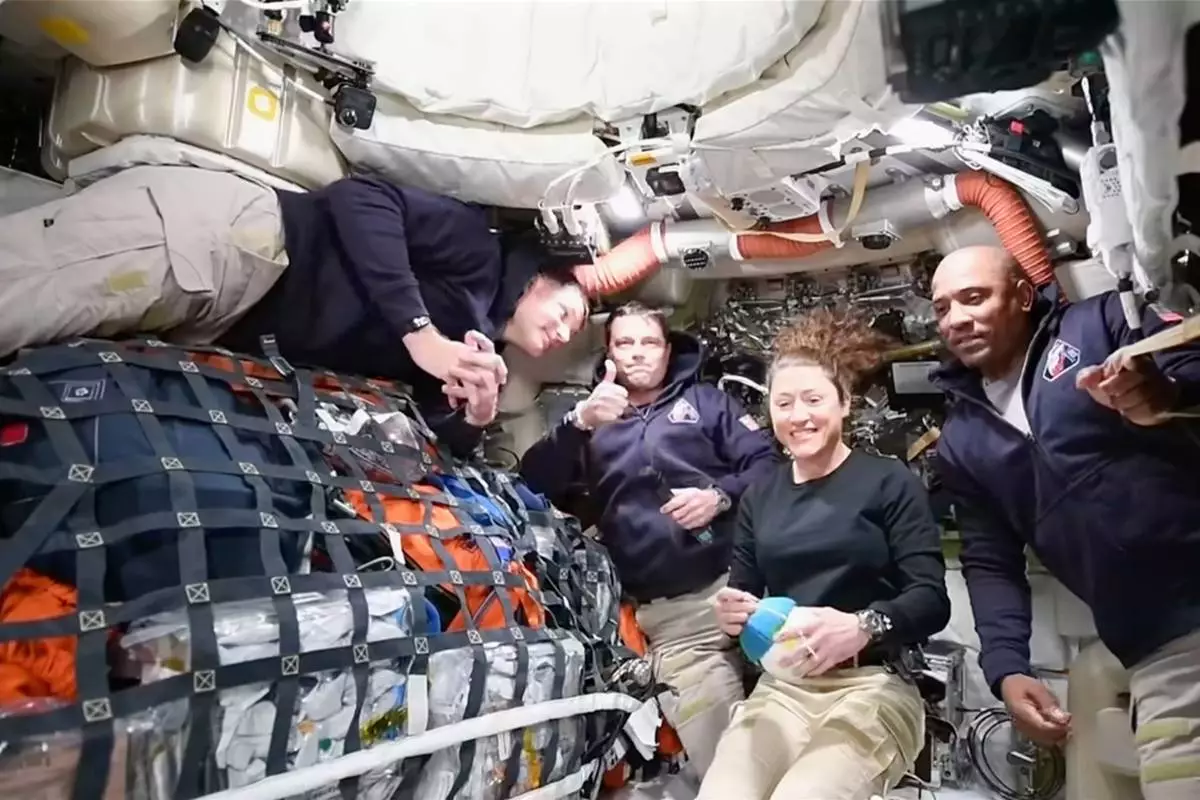
This image taken from video provided by NASA shows the Artemis II crew, from left, Canadien astronaut and mission specialist Jeremy Hansen, Commander Reid Wiseman, mission specialist Christina Koch and pilot Victor Glover as they speak with NASA Mission Control via video conference from the moon's orbit Thursday, April 2, 2026. (NASA via AP)
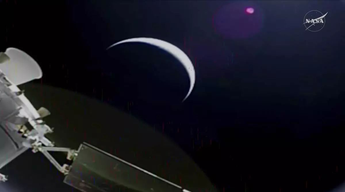
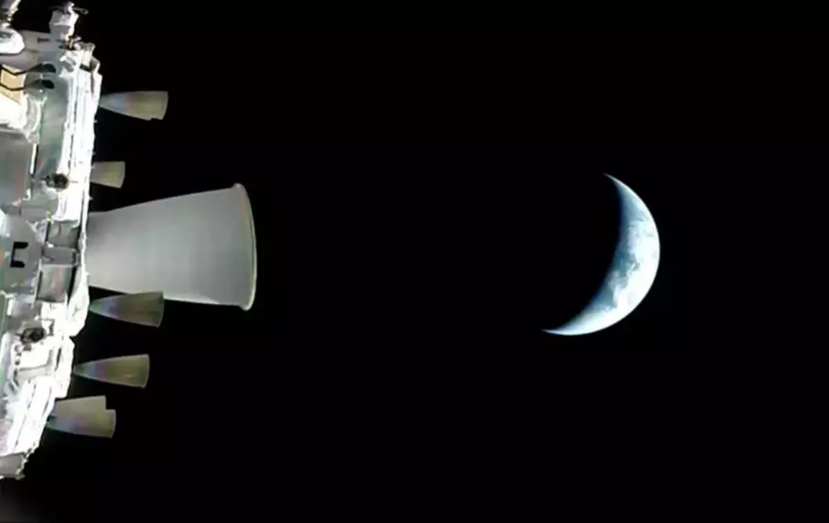
This image released by NASA on Thursday, April 2, 2026, shows NASA’s Orion spacecraft with Earth in the background. (NASA via AP)

This image taken from video provided by NASA shows the Earth, left, from NASA's Orion spacecraft as it fired its engines heading toward the moon Thursday, April 2, 2026. (NASA via AP)
In this photo provided by NASA, a view of the Earth from NASA's Orion spacecraft as it orbits above the planet during the Artemis II test flight, on Thursday, April 2, 2026. (NASA via AP)
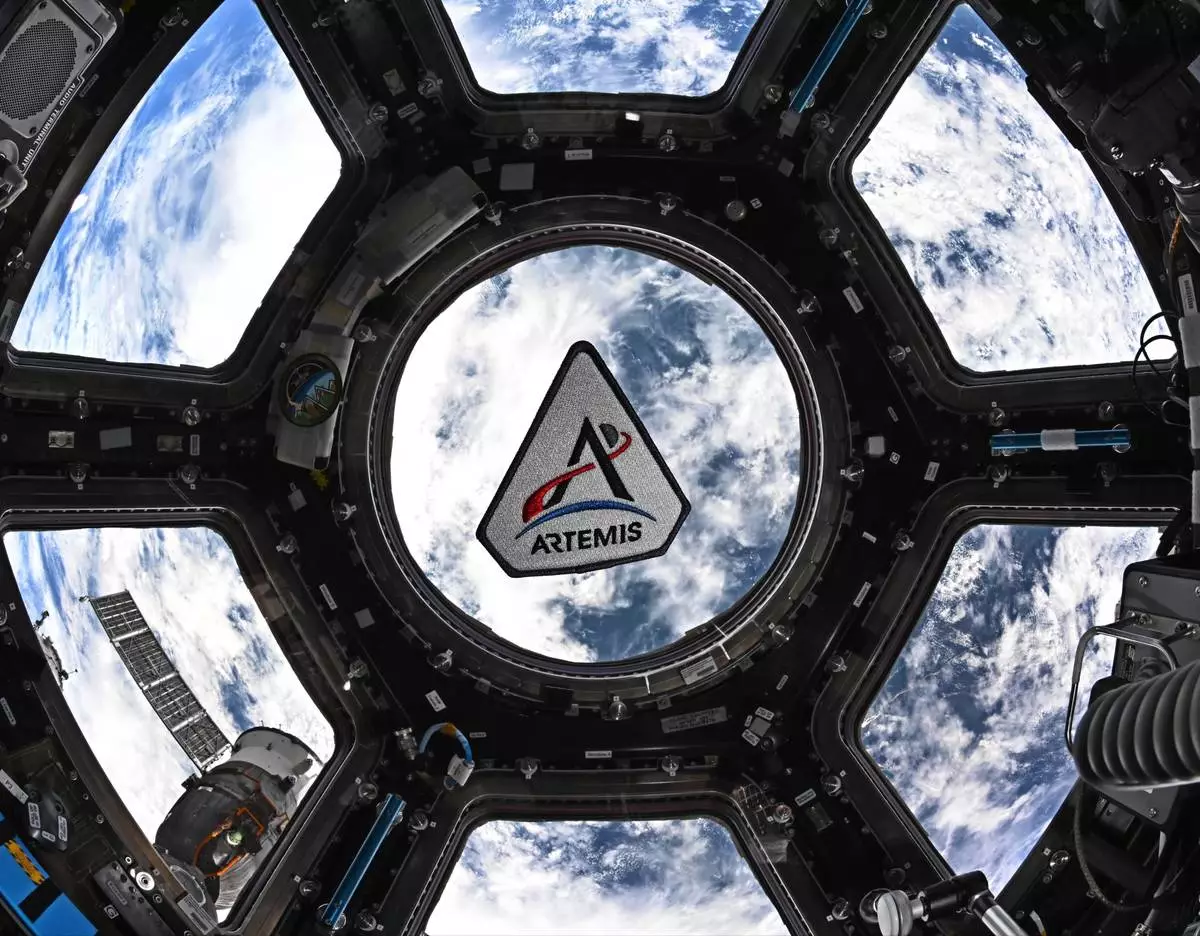
In this photo provided by NASA, an Artemis program patch floating in the International Space Station's cupola, on March 30, 2026. (Jessica Meir/NASA via AP)

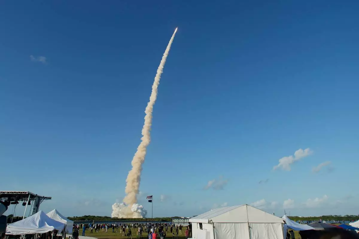
Spectators view NASA's Artemis II moon rocket launch from the A. Max Brewer Bridge, Wednesday, April 1, 2026, in Titusville, Fla. (AP Photo/Phelan M. Ebenhack)
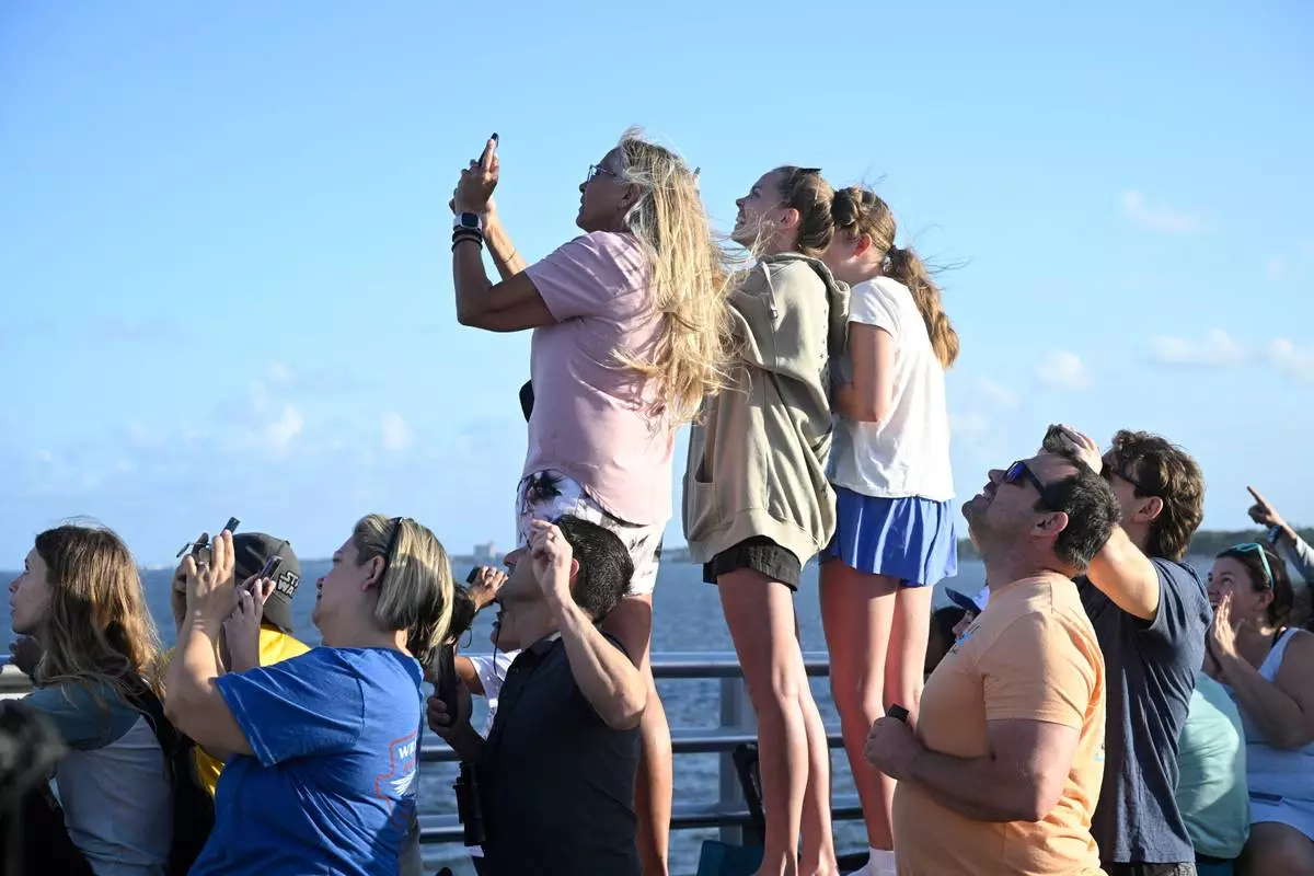
Spectators view NASA's Artemis II moon rocket launch from the A. Max Brewer Bridge, Wednesday, April 1, 2026, in Titusville, Fla. (AP Photo/Phelan M. Ebenhack)
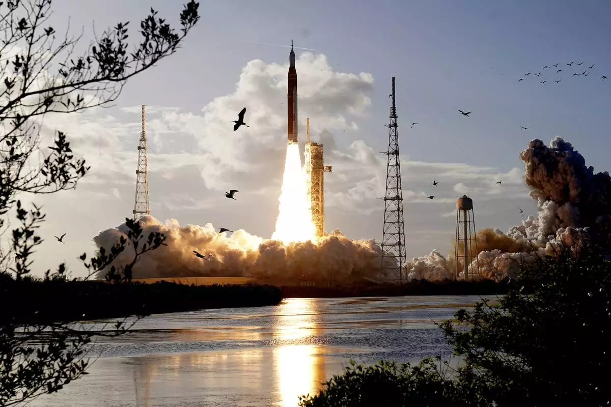
NASA's Artemis II moon rocket lifts off from the Kennedy Space Center's Launch Pad 39-B Wednesday, April 1, 2026, in Cape Canaveral, Fla. (AP Photo/Chris O'Meara)
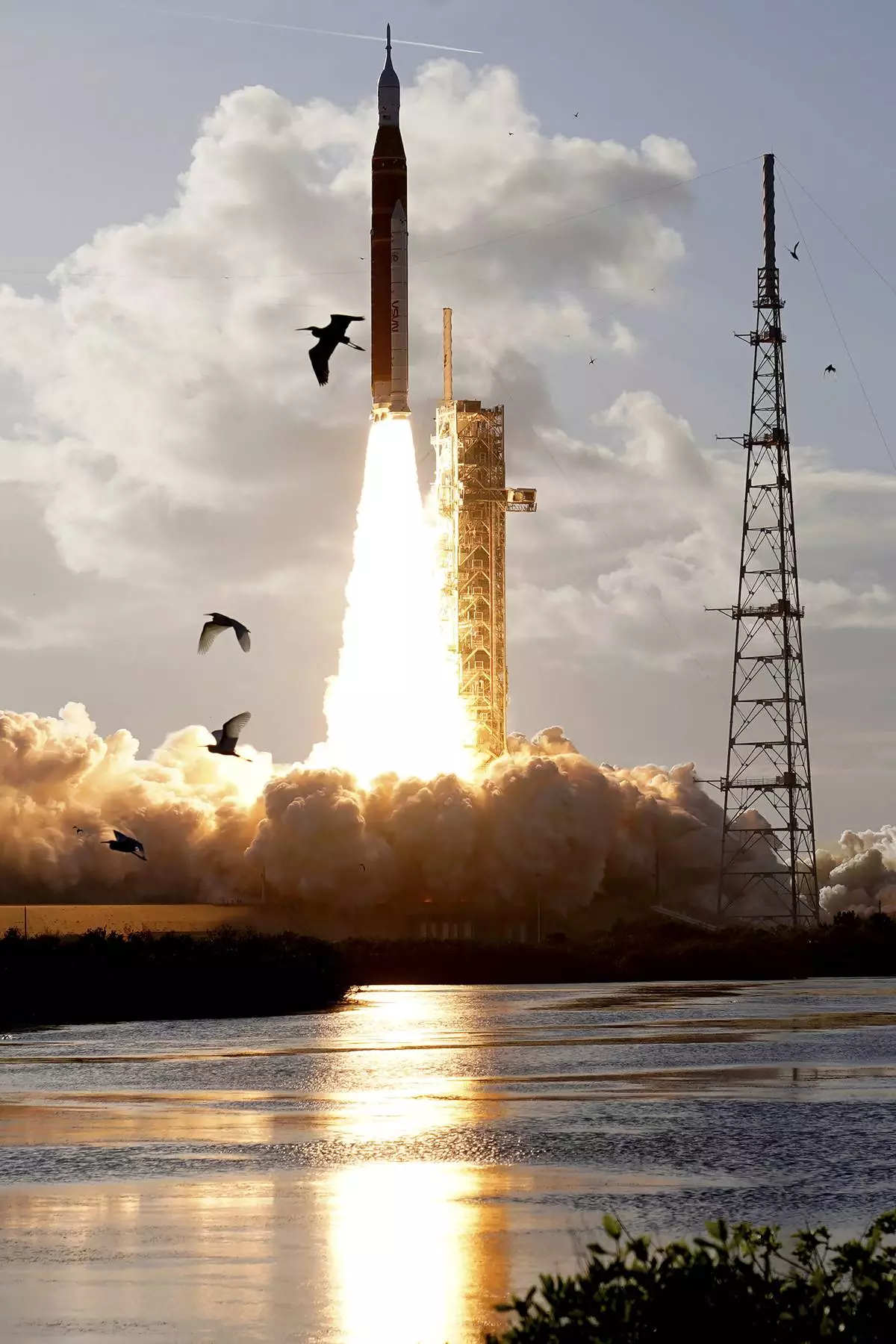
NASA's Artemis II moon rocket lifts off from the Kennedy Space Center's Launch Pad 39-B Wednesday, April 1, 2026, in Cape Canaveral, Fla. (AP Photo/Chris O'Meara)
NASA's Artemis II moon rocket lifts off from the Kennedy Space Center's Launch Pad 39-B Wednesday, April 1, 2026, in Cape Canaveral, Fla. (AP Photo/John Raoux)