KYOTO, Japan--(BUSINESS WIRE)--Apr 27, 2026--
Kyocera Corporation (President: Shiro Sakushima; “Kyocera”) today announced that it is commercializing a new multilayer ceramic core substrate for advanced semiconductor packages, such as xPUs (1) and switch ASICs, which are rapidly scaling in complexity as AI data center architectures evolve. The new product will be unveiled at ECTC 2026, an international conference on semiconductor packaging technologies, in Orlando, Florida, USA, May 26-29, 2026.
This press release features multimedia. View the full release here: https://www.businesswire.com/news/home/20260427129166/en/
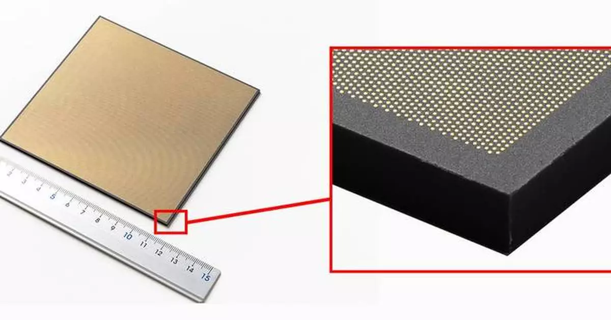
Built from Kyocera’s proprietary Fine Ceramic materials, the new core substrate is engineered for high‑density wiring and exceptional rigidity. According to the company, these characteristics dramatically reduce deformation (warpage) in high-performance semiconductor packages, a key challenge as demand for greater device integration and higher processing speed continues to rise.
(1): xPU is a general term for various processing units (PUs) such as CPUs and GPUs that handle AI processing.
Key Features
Development Background
The growth of generative AI and large language models is fueling a global proliferation of AI data centers and creating demand for higher-performance xPU and ASIC semiconductors that require larger, denser package substrates, especially for 2.5D packaging (2). Core substrates made of organic materials create a bottleneck to higher performance, especially at larger dimensions, due to warpage and wiring-miniaturization challenges. Kyocera is addressing these limitations with a new multilayer ceramic core substrate, leveraging its expertise in laminated ceramic materials to offer higher rigidity and finer wiring in advanced semiconductor packaging.
(2) 2.5D packaging refers to a structure in which multiple IC chips are placed side-by-side on a high-density interposer (relay substrate) using fine circuit patterning and vertical interlayer wiring to enhance processing speed.
Features
1. Highly rigid multilayer ceramic core substrate minimizes warpage, a key challenge affecting large package substrates
Kyocera’s multilayer ceramic core substrate provides greater rigidity and resistance to deformation (bending) than core substrates made of organic materials, minimizing warpage during each mounting phase. As a result, Kyocera’s multilayer ceramic technology can enable higher device performance using slimmer substrates (3) while facilitating further miniaturization.
(3): Based on Kyocera’s simulation results (February 2026).
2. Multilayer ceramic structure enables finer wiring
In multilayer ceramic substrates, conductive paths between layers of ceramic are called vias. Formed while the ceramic is pliable (before firing or sintering), these vias enable finer wiring through superior micro-fabrication as compared to the drilling processes used to create vias in conventional organic core substrates. The smaller via diameters and tighter via pitches made possible in ceramic substrates address the challenges associated with high-density wiring in traditional organic-core substrates.
3. Supports custom design requirements, and performance simulations in the design phase
During the design phase, Kyocera provides thermal, electrical, and substrate-warpage simulations based on device performance objectives and specified mounting processes. This simulation data ensures greater customer development efficiency and the achievement of design objectives in the finished device.
Kyocera remains committed to developing new packaging materials and technologies that meet evolving customer needs in the semiconductor industry.
About KYOCERA
Kyocera Corporation (TOKYO:6971, https://global.kyocera.com/ ), the parent and global headquarters of the Kyocera Group, was founded in 1959 as a producer of Fine Ceramics (also known as “advanced ceramics”). By combining these engineered materials with metals and integrating them with other technologies, Kyocera has become a leading supplier of ceramic components for a wide range of industries, as well as automotive components, semiconductor packages, electronic devices, smart energy systems, printers, copiers, and mobile phones. During the year ended March 31, 2025, the company’s consolidated sales revenue totaled 2.0 trillion yen (approx. US$13.2 billion). Kyocera appears on Forbes magazine’s 2025 “Global 2000” list of the world’s largest publicly traded companies, and has been named among “The World’s 100 Most Sustainably Managed Companies” by The Wall Street Journal. In January 2026, Kyocera was named to Clarivate’s list of the “Top 100” Global Innovators for the fifth consecutive year.
© 2026 Kyocera Corporation
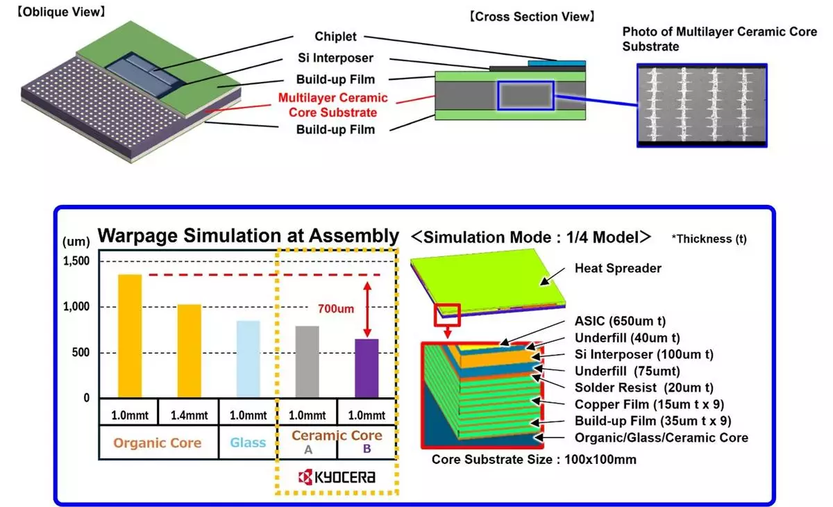
2.5D integration warpage comparison and simulation model
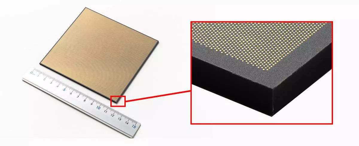
Multilayer ceramic core substrate for advanced semiconductor packaging