
MARLBOROUGH, Mass.--(BUSINESS WIRE)--Aug 20, 2026--
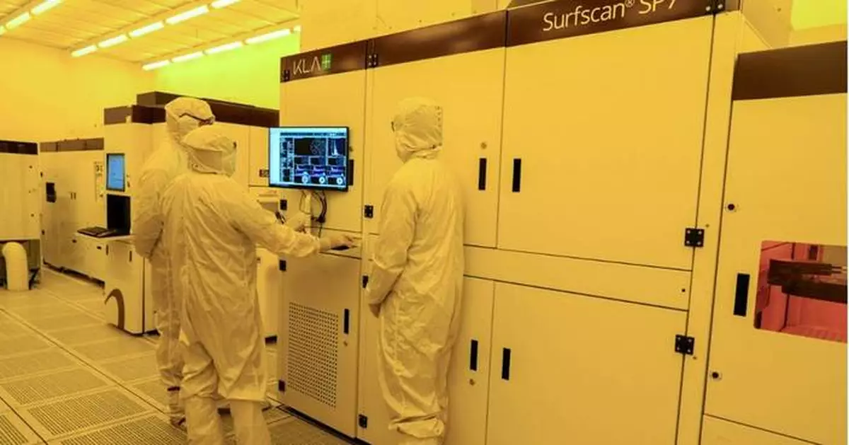
Qnity Electronics, Inc. (“Qnity”) (NYSE: Q), a premier technology solutions leader across the semiconductor value chain, today announced the installation of a Surfscan ® SP7 XP unpatterned wafer defect inspection system from KLA as part of its ongoing investment in advanced semiconductor materials innovation. The system enhances Qnity's ability to develop and manufacture leading-edge materials, deepening the process insight that supports customer technology roadmaps.
This press release features multimedia. View the full release here: https://www.businesswire.com/news/home/20260819307953/en/
“Developing breakthrough materials for advanced semiconductor technologies requires deep insight into performance and quality at every stage of development and manufacturing,” said Julia Woertink, VP of Technology, Semiconductor Technologies, Qnity. “By strengthening how we understand and control quality, we can help our customers push into more advanced nodes with greater confidence and speed.”
Installed at Qnity's New England Manufacturing & Technology Center in Marlborough, Mass., the Surfscan SP7 XP system is part of the company's broader investment strategy to support advanced semiconductor innovation across its global network. It expands Qnity's ecosystem of characterization and process control capabilities, helping teams identify sources of variation earlier in materials development and integration.
At advanced nodes, where even small defects can affect device performance, improved understanding of product and process variation supports faster process learning and scale-up for Qnity and its customers. Qnity’s latest investment supports the development and reliable manufacture of advanced lithography materials, including the Epic ® photoresist family for ArF lithography, the Eon™ photoresist family for extreme ultraviolet (EUV) lithography, and enabling underlayer materials.
“Qnity's investment in the Surfscan SP7 XP system reflects the growing emphasis on characterization and process control across the semiconductor value chain,” said James Seale, General Manager, KLA. “Process qualification, monitoring and defect characterization are key enablers for the quality and reliability required in advanced semiconductor applications.”
About Qnity
Qnity is a premier technology provider across the semiconductor value chain, empowering AI, high performance computing, and advanced connectivity. From groundbreaking solutions for semiconductor chip manufacturing, to enabling high-speed transmission within complex electronic systems, our high-performance materials and integration expertise make tomorrow’s technologies possible. More information about the company, its businesses and solutions can be found at www.qnityelectronics.com.
Qnity™ and the Qnity Node Logo are trademarks or registered trademarks of affiliates of Qnity Electronics, Inc. Surfscan ® is a registered trademark of KLA Corporation.
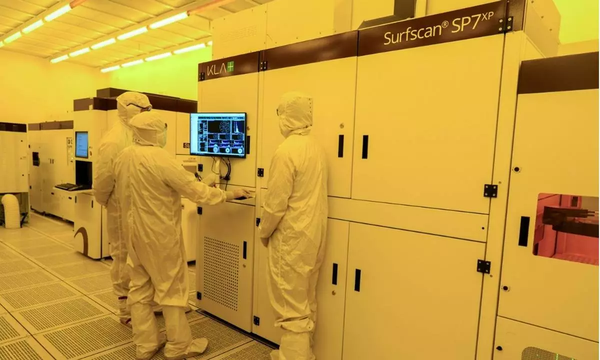
James Seale (left), general manager at KLA, joins Qnity's Besnik Cumani, fab equipment manager, and Drew Chambers, vice president and general manager of Lithography Technologies, in the fab at the Qnity New England Manufacturing & Technology Center in Marlborough, Mass., following the installation of a Surfscan® SP7XP unpatterned wafer defect inspection system from KLA. The system supports Qnity's ongoing investment in advanced semiconductor materials innovation.